- 您现在的位置:买卖IC网 > Sheet目录685 > D75F-013.0M (Connor-Winfield)OSC TCXO 13.000 MHZ 3.3V SMD
�� �
�
�2111� Comprehensive� Drive�
�Aurora,� Illinois� 60505�
�Phone:� 630-� 851-� 4722�
�Fax:� 630-� 851-� 5040�
�www.conwin.com�
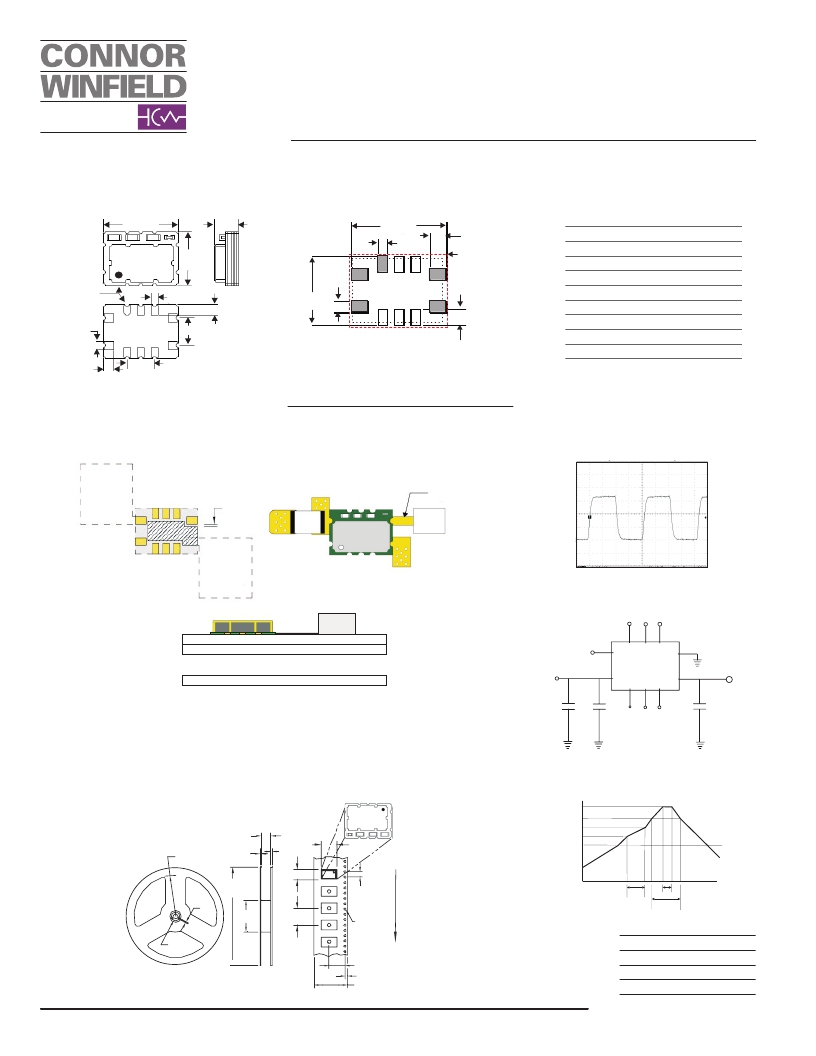
�Package� Layout�
�Suggested� Pad� Layout�
�Pad� Connections�
�D75F� 1144�
�0.040�
�2�
�3�
�1�
�4�
�Bottom�
�0.100�
�60� to� 90� s�
�Typical�
�View�
�±.005� (.127mm)�
�Top� View�
�10�
�4�
�Pin 1�
�0.030�
�(0.762mm)�
�(4� Places)�
�0.038�
�(0.965mm)�
�(4� Places)�
�10�
�9�
�0.079� Max.�
�0.276� ±� 0.006�
�(2.0mm)�
�(7.0mm)�
�0.197�
�±� 0.006�
�27.0� MHZ� (5.0mm)�
�0.025(6� Places)�
�(0.635mm)�
�(1.02mm)�
�(6� Places)�
�Temperature�
�260°C�
�260°C�
�220°C�
�180°C�
�150°C�
�120°C�
�0�
�10� s�
�Up� to� 120� s�
�Typical�
�Meets� IPC/JEDEC� J-STD-020C�
�(2.54mm)�
�5�
�8� 7� 6�
�Dimensional� Tolerance:�
�0.100�
�(2.54mm)� ±.02� (.508mm)�
�0.295�
�(7.49mm)�
�0.051�
�0.030� (1.28mm)�
�(0.76mm)�
�Keep� Out� Area�
�8� 7� 6�
�0.037� 9� 5�
�(0.94mm)�
�0.215�
�(5.46mm)�
�0.051�
�1� 2� 3� (1.28mm)�
�*� Do� not� route� any� traces� in� the� keep� out� area.� It� is�
�recommended� the� next� layer� under� the� keep� out�
�area� is� to� be� ground� plane.�
�1:�
�2:�
�3:�
�4:�
�5:�
�6:�
�7:�
�8:�
�9:�
�10:�
�Do� Not� Connect�
�Do� Not� Connect�
�Do� Not� Connect�
�Ground�
�Output�
�Do� Not� Connect�
�Do� Not� Connect�
�Tri-State� Enable� /� Disable�
�Supply� Voltage� Vcc�
�N/C�
�Vcc,� should� have�
�a� large� copper�
�Design� Recommendations�
�Output� Waveform�
�area� for� reduced�
�inductance.�
�Connect� a� 0.01uF�
�bypass� capacitor�
�0.010”(0.254mm)�
�Recommended�
�clearance�
�Vcc�
�50� Ohm� trace�
�<1”by� design�
�<0.1”(2.54mm)�
�from� the� pad.�
�9�
�10�
�8�
�1�
�6�
�3�
�5�
�4�
�inductance�
�for� internal�
�copper� flood.�
�Ground,�
�Ground�
�Buffer�
�Top� View�
�should� have�
�a� large� copper�
�Top� View�
�Ground�
�1V/Div�
�area� for� reduced�
�inductance.�
�50� Ohm� Trace�
�Test� Circuit�
�OSC�
�Without�
�Output�
�DNC�
�DNC� DNC�
�TOP� LAYER�
�Vias�
�Buffer�
�GROUND� LAYER�
�N/C�
�10�
�1�
�2�
�3�
�4�
�Ground�
�Vcc�
�BOTTOM� LAYER�
�Supply�
�Voltage�
�9�
�8�
�7�
�6�
�5�
�Output�
�Attention:� To� achieve� optimal� frequency� stability,� and� in� some� cases� to� meet� the� specification� stated� on� this� data�
�sheet,� it� is� required� that� the� circuit� connected� to� this� TCXO� output� must� have� the� equivalent� input� capacitance�
�that� is� specified� by� the� nominal� load� capacitance.� Deviations� from� the� nominal� load� capacitance� will� have� a�
�graduated� effect� on� the� stability� of� approximately� 20� ppb� per� pF� load� difference.�
�0.1� uF�
�Bypass�
�10� nF�
�Bypass�
�Enable/� DNC� DNC�
�Disable�
�DNC� =� Do� Not� Connect�
�15� pF�
�Tape� and� Reel� Dimensions�
�Solder� Profile�
�PIN� 1�
�Temperature�
�260°C�
�220°C�
�180°C�
�260°C�
�8.46� DIA�
�(216mm� DIA)�
�.69�
�(17.5mm)�
�.08�
�(2.0mm)�
�.08�
�(2.0mm)�
�.31�
�(7.9mm)�
�150°C�
�120°C�
�60� to� 90� s�
�Typical�
�.08�
�(2.0mm)�
�9.84� DIA�
�(250mm� DIA)�
�3.15�
�(80mm)�
�.21�
�(5.4mm)�
�.315�
�(8.0mm)�
�.157�
�(4.0mm)�
�.06� DIA�
�(1.5mm� DIA)�
�Direction�
�Of�
�Feed�
�(Customer)�
�0�
�10� s�
�Up� to� 120� s�
�Typical�
�Meets� IPC/JEDEC� J-STD-020C�
�1.00� DIA�
�(25mm� DIA)�
�MEETS� EIA-481A� and� EIAJ-1009B�
�2,000� PCS/REEL�
�.295� (7.5mm)�
�.07� (1.75mm)�
�.83� (16.0mm)�
�Bulletin�
�Page�
�Revision�
�Date�
�Tx237�
�2� of� 2�
�03�
�03� Dec� 2013�
�Specifications� subject� to� change� without� notification.� See� Connor-Winfield's� website� for� latest� revision.� All� dimensions� in� inches.�
�?� Copyright� 2014� The� Connor-Winfield� Corporation�
�Not� intended� for� life� support� applications.�
�发布紧急采购,3分钟左右您将得到回复。
相关PDF资料
D75J-040.0M-T
TCXO 40.00000 MHZ 3.3V LVCMOS
D7G0511S
SWITCH ROTARY 5P-11POS OPEN FRM
D8G0817N
SWITCH ROT 8P 2-17 ACTIVE POS
D9G0723N
SWITCH ROTARY 7P-23POS OPEN FRM
DA12T
RIGHT-ANGLE DIP SWITCH
DEA102500LT-6307A1
FILTER LOW PASS 2.45GHZ SMD
DEA160915LT-1169
FILTER LOWPASS AGSM-EGSM/TX SMD
DEA161990LT-1182
FILTER LOWPASS PCS/TX-RX SMD
相关代理商/技术参数
D75F-013.0M-T
功能描述:OSC TCXO 13.000 MHZ 3.3V SMT RoHS:是 类别:晶体和振荡器 >> 振荡器 系列:D75F 标准包装:1 系列:VG-4512CA 类型:VCXO 频率:153.6MHz 功能:三态(输出启用) 输出:LVPECL 电源电压:3.3V 频率稳定性:- 工作温度:-40°C ~ 85°C 电流 - 电源(最大):60mA 额定值:- 安装类型:表面贴装 尺寸/尺寸:0.276" L x 0.197" W(7.00mm x 5.00mm) 高度:0.071"(1.80mm) 封装/外壳:6-SMD,无引线(DFN,LCC) 包装:Digi-Reel® 电流 - 电源(禁用)(最大):- 其它名称:SER3790DKR
D75F-019.44M
功能描述:OSC TCXO 19.440 MHZ 3.3V SMD RoHS:是 类别:晶体和振荡器 >> 振荡器 系列:D75F 标准包装:1 系列:VG-4512CA 类型:VCXO 频率:153.6MHz 功能:三态(输出启用) 输出:LVPECL 电源电压:3.3V 频率稳定性:- 工作温度:-40°C ~ 85°C 电流 - 电源(最大):60mA 额定值:- 安装类型:表面贴装 尺寸/尺寸:0.276" L x 0.197" W(7.00mm x 5.00mm) 高度:0.071"(1.80mm) 封装/外壳:6-SMD,无引线(DFN,LCC) 包装:Digi-Reel® 电流 - 电源(禁用)(最大):- 其它名称:SER3790DKR
D75F-019.44M-T
功能描述:OSC TCXO 19.440 MHZ 3.3V SMT RoHS:是 类别:晶体和振荡器 >> 振荡器 系列:D75F 标准包装:1 系列:VG-4512CA 类型:VCXO 频率:153.6MHz 功能:三态(输出启用) 输出:LVPECL 电源电压:3.3V 频率稳定性:- 工作温度:-40°C ~ 85°C 电流 - 电源(最大):60mA 额定值:- 安装类型:表面贴装 尺寸/尺寸:0.276" L x 0.197" W(7.00mm x 5.00mm) 高度:0.071"(1.80mm) 封装/外壳:6-SMD,无引线(DFN,LCC) 包装:Digi-Reel® 电流 - 电源(禁用)(最大):- 其它名称:SER3790DKR
D75F-025.0M
功能描述:OSC TCXO 25.000 MHZ 3.3V SMD RoHS:是 类别:晶体和振荡器 >> 振荡器 系列:D75F 标准包装:1 系列:VG-4512CA 类型:VCXO 频率:153.6MHz 功能:三态(输出启用) 输出:LVPECL 电源电压:3.3V 频率稳定性:- 工作温度:-40°C ~ 85°C 电流 - 电源(最大):60mA 额定值:- 安装类型:表面贴装 尺寸/尺寸:0.276" L x 0.197" W(7.00mm x 5.00mm) 高度:0.071"(1.80mm) 封装/外壳:6-SMD,无引线(DFN,LCC) 包装:Digi-Reel® 电流 - 电源(禁用)(最大):- 其它名称:SER3790DKR
D75F-025.0M-T
功能描述:OSC TCXO 25.000 MHZ 3.3V SMT RoHS:是 类别:晶体和振荡器 >> 振荡器 系列:D75F 标准包装:1 系列:VG-4512CA 类型:VCXO 频率:153.6MHz 功能:三态(输出启用) 输出:LVPECL 电源电压:3.3V 频率稳定性:- 工作温度:-40°C ~ 85°C 电流 - 电源(最大):60mA 额定值:- 安装类型:表面贴装 尺寸/尺寸:0.276" L x 0.197" W(7.00mm x 5.00mm) 高度:0.071"(1.80mm) 封装/外壳:6-SMD,无引线(DFN,LCC) 包装:Digi-Reel® 电流 - 电源(禁用)(最大):- 其它名称:SER3790DKR
D75F-027.0M
功能描述:OSC TCXO 27.000 MHZ 3.3V SMD RoHS:是 类别:晶体和振荡器 >> 振荡器 系列:D75F 标准包装:1 系列:VG-4512CA 类型:VCXO 频率:153.6MHz 功能:三态(输出启用) 输出:LVPECL 电源电压:3.3V 频率稳定性:- 工作温度:-40°C ~ 85°C 电流 - 电源(最大):60mA 额定值:- 安装类型:表面贴装 尺寸/尺寸:0.276" L x 0.197" W(7.00mm x 5.00mm) 高度:0.071"(1.80mm) 封装/外壳:6-SMD,无引线(DFN,LCC) 包装:Digi-Reel® 电流 - 电源(禁用)(最大):- 其它名称:SER3790DKR
D75F-027.0M-T
功能描述:OSC TCXO 27.000 MHZ 3.3V SMT RoHS:是 类别:晶体和振荡器 >> 振荡器 系列:D75F 标准包装:1 系列:VG-4512CA 类型:VCXO 频率:153.6MHz 功能:三态(输出启用) 输出:LVPECL 电源电压:3.3V 频率稳定性:- 工作温度:-40°C ~ 85°C 电流 - 电源(最大):60mA 额定值:- 安装类型:表面贴装 尺寸/尺寸:0.276" L x 0.197" W(7.00mm x 5.00mm) 高度:0.071"(1.80mm) 封装/外壳:6-SMD,无引线(DFN,LCC) 包装:Digi-Reel® 电流 - 电源(禁用)(最大):- 其它名称:SER3790DKR
D75F271J03
制造商:未知厂家 制造商全称:未知厂家 功能描述:Miniature Dipped, Mica Capacitors